Plasmonics for Sustainable Energy
 Surface Plasmons for Photovoltaics
Surface Plasmons for Artificial Photosynthesis
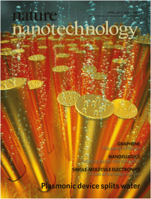
In plasmonics we have two major goals: the first is to create plasmonic analogs of photovoltaics and photosynthetic systems. Recently, for example, we produced the first device ever reported which uses the electrons resulting from the decay of plasmons in gold nanorods to reduce hydrogen ions in water, and the positive charges left behind to oxidize water to oxygen gas. The device is a free running cell floating in water with light as its sole energy source. (Surface plasmons are collective conduction electron excitations that occur in nanostructured metals and some other conductors.)
SERS for Biosensing
 Cancer Detection
Intracellular pH Sensing
SERS Based Immunoassay
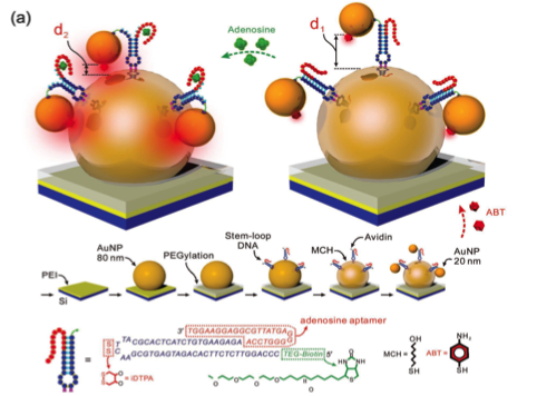
SERS is also a plasmonic phenomenon. The excitation of plasmons concentrate electromagnetic radiation in nanometer-sized volumes – so-called hot spots. Molecules located in such hot spots can produce enormously enhanced spectra. Collaborating with colleagues in engineering, and especially the group of Professor Carl Meinhart, we pursue a number of research avenues often by combining microfluidics with SERS spectroscopy. For example, we have created very bright nanotags that can contain a peptide or an aptamer that can interact either with an analyte or the surface of a cell. The very bright SERS spectrum of the nanotag is then used to pick out, for example, cancer cells from among non-cancerous cells flowing in the microfluidic stream; or to detect and identify small analyte molecules at very low concentrations entering the microfluidic stream from the ambient atmosphere.
Nanoelectronics
 Nanowire Based Electronic Nose
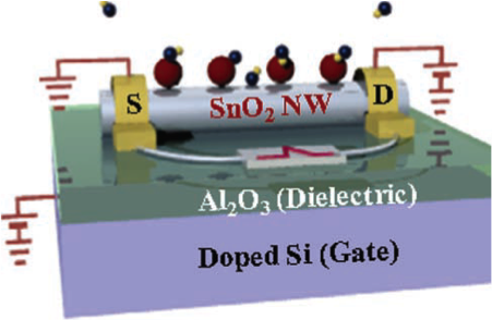
Our research work with semiconductor nanowires attempts to understand the transduction process that converts chemical events at the surface of nanowires, and especially nanowires functionalized with catalytic nanoparticles, to the electrical conductivity of the nanowire. Most often such nanowires are configured as field-effect transistors and the Gate voltage, that controls the electric field across the nanowire, is used to tune the nanowire’s “chemical potential”, thereby providing what is in essence an electronic means for functionalizing the nanowire’s surface.
